- NTAG216 = a manufacturer's model number, sort of
- chip = integrated circuit
- from = I ripped the thing apart to see what was inside
- NFC = Near Field Communications
- RFID = Radio Frequency IDentification
- label = thin flat sticky thing
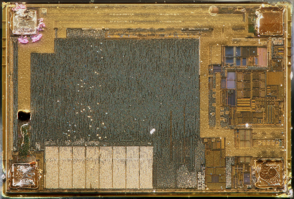
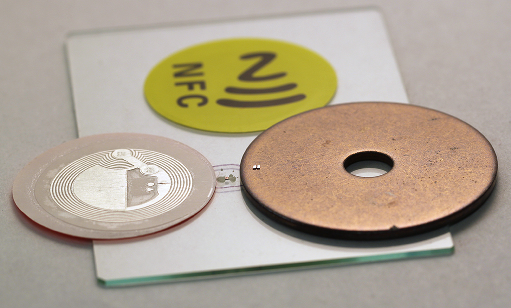
Various views and pieces. The glass slide is 2" wide. The metal washer with the shiny thing sitting on it is part of the setup that I used to burn away the plastic and epoxy. The shiny thing on the washer is mostly a small portion of the antenna coil, with the chip still sitting under the two pieces of antenna that are now only tenuously attached to it. The fully cleaned chip that is shown in the first image is glued to the slide between the washer and the label. You'll have to look close, because in this image the chip itself is only about 5 pixels square.
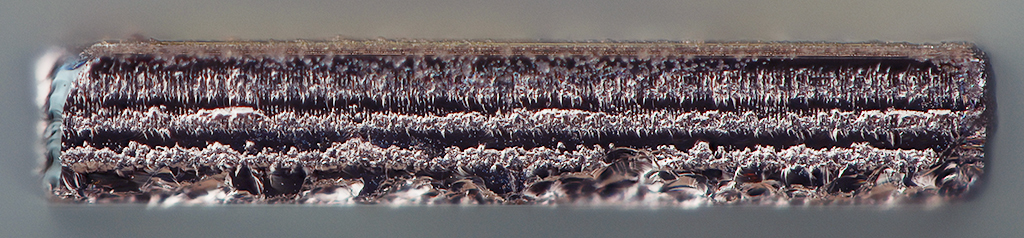
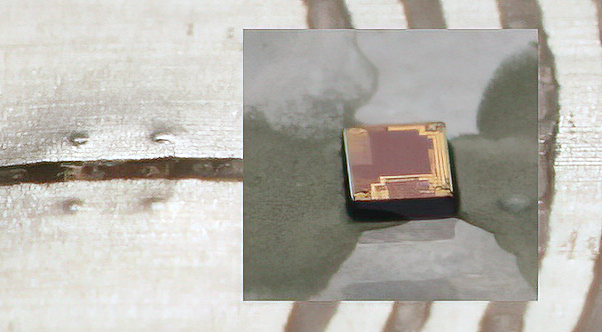
Zooming in closer, plus some montaging, this is the decapsulated chip sitting next to its sibling which is still fully functional inside the label. You can see that the antenna coil is split and is bonded to the chip in all four corners. It turns out that two of those bonds are only mechanical at this point. When manufactured, the chip has four electrical connections, two for the antenna and two more for GND and TP. But the manufacturer's documentation at https://www.nxp.com/docs/en/data-sheet/ ... 15_216.pdf makes clear that "Pads GND and TP are disconnected when wafer is sawn."
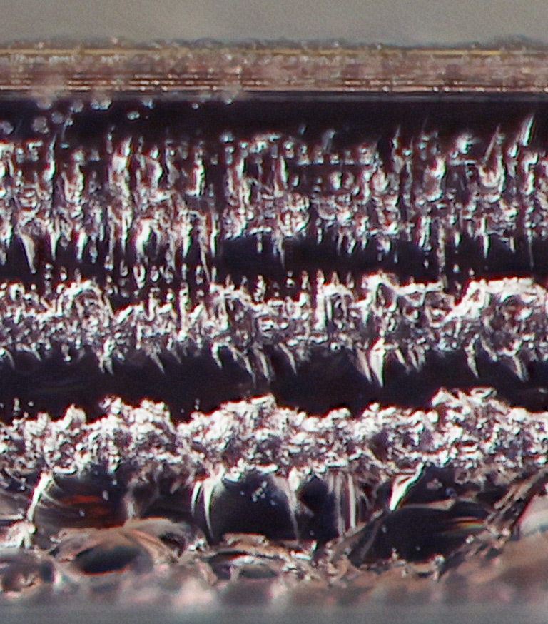
This chip is particularly interesting to me because portions of it have richly detailed 3D structure. Here are a couple of stereo pairs at high magnification, cropped in so that the structure is easier to see. These are Zerene Stacker synthetic stereo at +-8 degrees, so 16 degrees total stereo separation. I want to say that this exaggerates the 3D structure, compared to what you'd see through a stereo scope, but these structures are so small that with my stereo scope they're basically invisible even at 45X. These were shot at 20X NA 0.42, same as the image at top of post, but here we are strongly zoomed in by cropping.
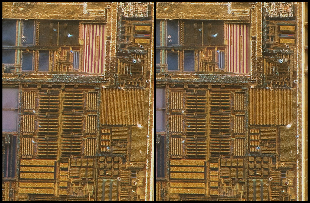
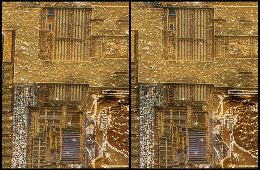
In offline communications I've been asked how I photograph these things. Photographing flat at this magnification often makes a mess because the only light that gets into the objective is what bounces off the edges of 3D structures. The structure looks a lot better if the flat surfaces are illuminated also. That could be done with through-the-lens illumination ("episcopic brightfield"), but the trick I use is to just tip the chip a little (about 8 degrees), so that some diffuse illumination can get around the objective, bounce off the mirrored surfaces of the chip, and still get into part of the objective. The light does not get into the whole objective, which causes some strange apparent lateral movements that depend on focus, even though no physical lateral movement happens.. But the stacking process sorts it out pretty well, so we end up with good images in the end.
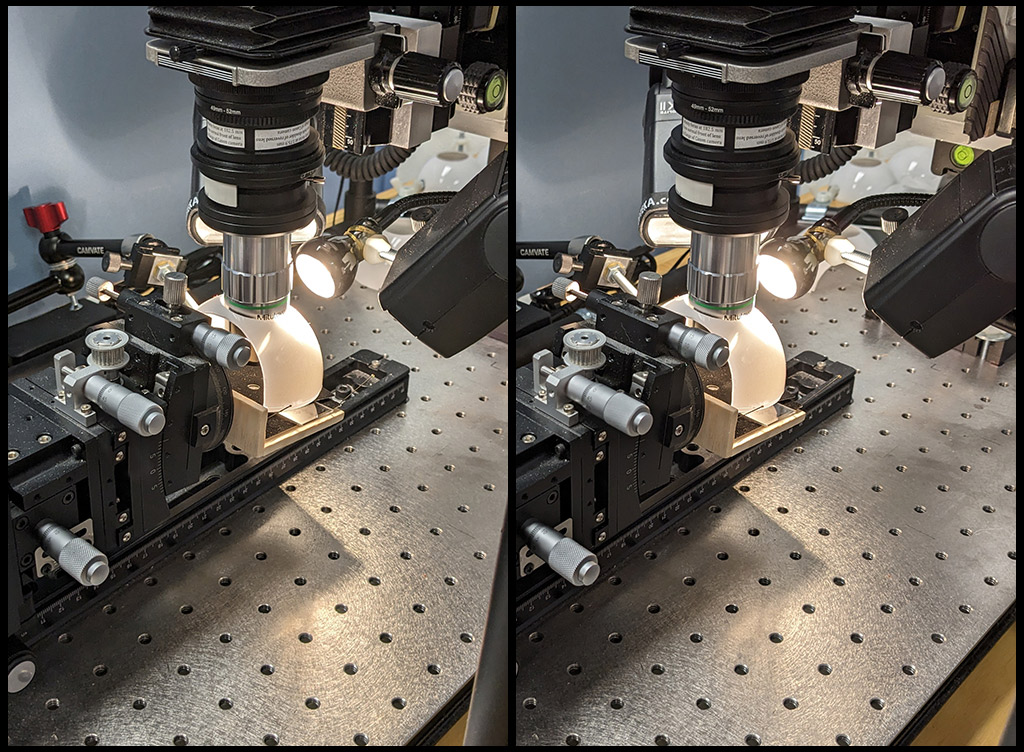
Here is a stereo pair showing the setup. This pair is shot using cha-cha technique with a cell phone, then run through StereoPhoto Maker for alignment and cropping. I was surprised at how simple and effective this technique turns out to be. Just maneuver my head into position so that my real eyes can see what they want, then position the camera of the cell phone directly in front of each eye while taking the shot. I can get the cell phone aligned with my eyes to within a few mm, so this really is a matter of what-I-saw-is-what-I-got. In this image the chip is sitting in the middle of the circular hole punched in black velvet paper that suppresses reflections from the rest of the glass slide. Careful positioning of my head was required so that both eyes could see the chip, and that positioning was nicely preserved in the images captured by camera.
--Rik
More details: Canon R7 camera, Mitutoyo DCR-150 tube lens, Mitutoyo M Plan Apo 20X NA 0.42, focus-stepped at 1 micron. Decapsulated by 10 minutes burn-off, held between washers sitting on a red-hot electric heating coil, then ultrasonically cleaned after cooling.