chris_ma wrote:mawyatt wrote:Really nice chip image, and beautiful chip subject with great colors!! Most of the wafers/chips I've purchased are kinda mundane compared to this chip! Are these specific chips still available?
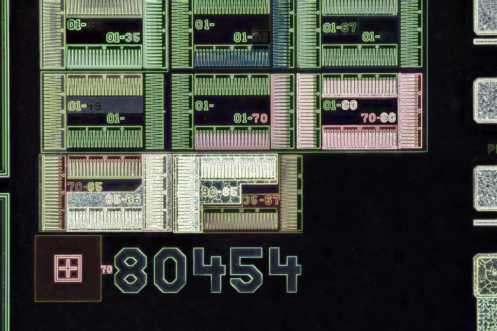
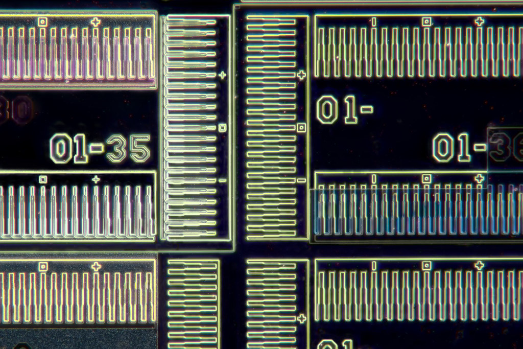
The chip size, looks to be ~2.6mm by 2.3mm if those are 100um bond pads.
i think it's this chip:
https://www.ebay.de/itm/100pcs-Toshiba- ... 3743175642
description says 2.5x2.5m, so pretty much spot on with your estimate.
free shipping world wide.
what's more, I think I have some of those... somewhere - gotta go digging

Yeah, exactly the same, the one you linked has the information on the tray, thanks for that! I paid $1 each for my trays, these are so cheap on Chinese websites.
Lou Jost wrote:Macro_cosmos, I also have a 40-50 of those, or something similar. They are useful but much better would be a complete wafer with chips all over.
My initial idea was to 3D print a tray tailored to fullframe sensors and embed these chips in the tray, allowing me to place them in the centre, border (APS-C) then corners. I ditched the idea after getting photomasks.
It's totally possible for all of us to come together and design a mask that has all the information we want. I know someone who can make these masks down to a resolution of 0.1um. 1um would be a lot cheaper.
Some stuff include
- dotted pattern and grid for distortion
- ruler for magnification
- Slanted edge for MTF
- Various diffraction gratings for resolution/sharpness
I'm just not sure how much it will cost. It depends on how many are interested. With these things, it's always quantity. More units means considerably cheaper and faster lead time.